

Introduction
In the previous blog, we discussed how voltage glitching can be used to bypass Read Protection on STM32F4 series MCUs. In this blog, we describe the security research performed on an Automotive ECU, where we extracted the firmware by performing a voltage glitching attack. The target ECU featured a Renesas RH850/F1L series MCU with protected debug access.
Target Reconnaissance
The target device under consideration for this security research is a Body Control Module (BCM) Automotive ECU. BCM in a vehicle is responsible for controlling the power windows/mirrors, immobilizer system, central locking, etc. The main objective of this security research was to extract the firmware from the ECU and obtain any confidential information such as secret keys etc. We tried to extract memory contents through CAN interface, but it was protected with security access.
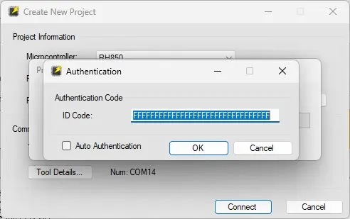
Next, we disassembled the ECU to analyze the PCB and its components. The ECU contains RH850/F1L series MCU from Renesas. We first checked if there was any open debug port available. Using Renesas E1 debugger and a bit of soldering, we established connectivity with the target device via the JTAG Pins and the tester PC. We followed the steps mentioned in Renesas Flash Programmer User Manual, which prompted us to enter the 16 bytes ID Code as shown below.
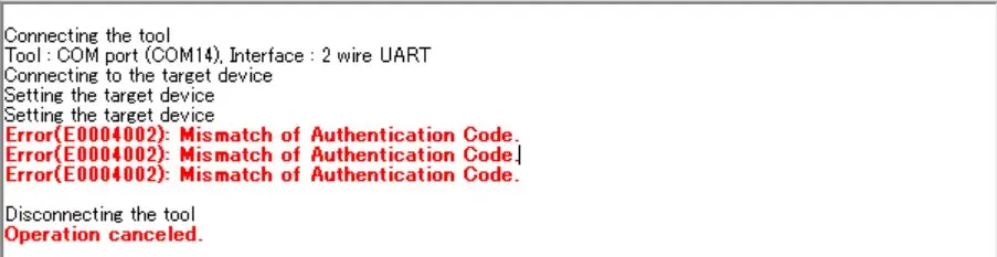
We tried some commonly used codes but were unsuccessful which resulted in an error message indicating “Mismatch of Authentication Code”.
Fault Injection to Bypass Debug Protection
Since the debug access was locked, a potential way to bypass it was through fault injection attack. There are lot of research publicly available, where fault injection attacks were used to bypass debug protection. There were some fault injection attacks carried out especially on Renesas MCUs, one of them is by Willem Melching on an automotive ECU, where the serial programming interface itself was disabled but was successfully bypassed through fault injection. Our target is a bit different as the serial programming is not disabled but is protected by an ID Code Authentication. The other research is by Franck Jullien’s on Renesas RX65, where the architecture, boot ROM and debug protocol (single-wire FINE) is different as compared to RH850.
The datasheet indicated the MCU has 3 operating modes, out of which one is the Serial Programming Mode. The settings to enable the Serial Programming mode is mentioned in the datasheet. FLMD0 pin was pulled high to enable serial programming mode for our target.
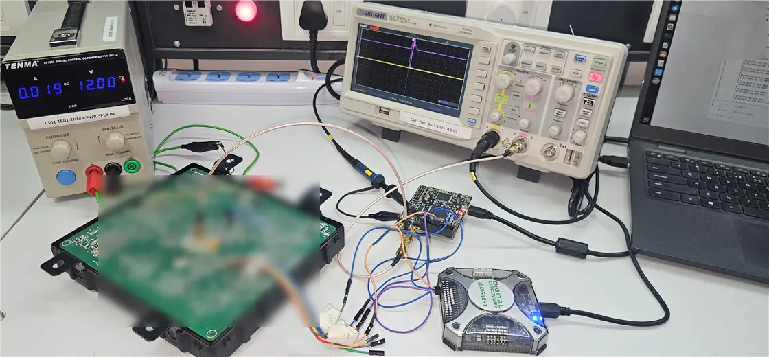
As mentioned in this document RH850 uses 2 wire UART for serial connection. The connection diagram for the same is mentioned here. We used USB to serial converter to connect to our target. We also hooked up a logic analyser to analyse the communication between the Renesas Flash Programmer and the target device.
The serial programming mode is of interest to us because decoding serial communication commands is way easier and will help us to understand how the debug protocol works as well as find any potential vulnerabilities. This will also enable us to develop the software for fault injection.
2 Wire UART - Protocol Analysis
As mentioned above RH850 uses 2 Wire protocol in serial programming mode. We hooked up a logic analyser to the communication lines and analysed the communication between the PC and target while trying to connect to the target via the Renesas Flash Programmer GUI. We performed all of the operations mentioned in the RFP User Manual and analysed the communication.
The following were our observations:
The communication is the form of commands which have a predefined packet structure.
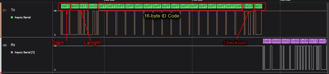
Each command starts with 0x81 or 0x01 byte, followed by the length of the command.
Each command ends with a constant 0x03, preceded by a 1 byte checksum.
The RFP tool sends and receives a series of commands among which the main commands are described below:
- The RFP tool first sends a series of zeros to see if the device responds.
- Next the RFP tool requests for the device info, maximum and minimum input frequency, maximum and minimum system clock frequency supported by the MCU.
- RFP tool then sends the main clock frequency set by the User.
- Setting the bitrate (9600) for the serial communication.
- Check if the serial programming is enabled.
- If the serial programming is enabled, the RFP tool sends the 16-byte ID Code entered by the user.
The below figure shows the ID Code Check command where the 16-byte password entered by the user (all FFs) is transferred over the serial lines.
We obtained a RH850 dev board and read the memory (Code flash and Data Flash) to understand the commands for the same, which is usually performed after the ID Code Authentication is successful. Once the positive response is obtained, the RFP tool reads the device ID, and it proceeds to read memory from the user specified area. One thing which we observed is that the memory is read in chunks. The RFP tool sends the start and end memory address from where the data needs to be read. Once the data is received, the address is incremented, and the command is sent again.
RH850 Power Supply Circuit
For Voltage Glitching attack, we need to target the power supply of the MCU. Every MCU has a specifically designed power management/regulation system, which is used for powering the internal circuitry, peripherals etc. The power supply scheme of RH850/F1L is shown in the below figure.
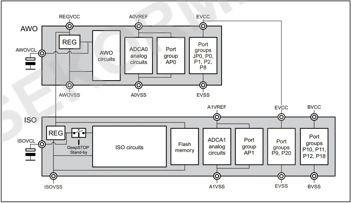
The MCU internal circuits are separated into two independent power domains, the Always-On area (AWO) and the Isolated area (ISO). Each power domain has a separate voltage regulator. From the power supply scheme, it is clear that AWOVCL and ISOVCL pins gives us direct access to internal voltage regulators. These two points can be considered as glitch injection points to inject faults into the system.
We chose ISOVCL as the glitch injection points because as per the power supply scheme ISOVCL is responsible for power management of the flash memory.
Glitch Setup
Hardware Setup
Every system has components designed to specifically maintain its operating voltage at the appropriate levels, such as decoupling capacitors. One of the challenges/requirements with voltage glitching is to modify/tamper with the hardware circuitry to overcome the protection offered by these components. This includes removal of some components or replacing them with custom components, as well as selecting the glitch injection point.
As mentioned above we selected ISOVCL as the glitch injection point. The decoupling capacitors on ISOVCL were replaced, which would increase the impact of our glitch on the target. The values of which were chosen following comprehensive research to ensure desired glitch is obtained.
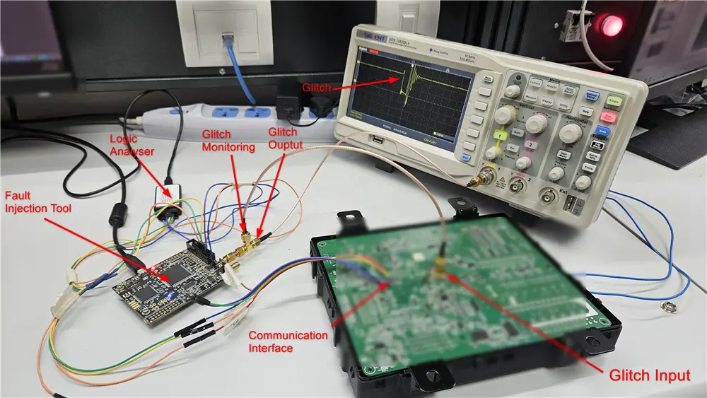
We used Chipwhisperer Lite (CW) to generate the glitch required for our target. The glitcher software on Chipwhisperer Lite communicates to the target serially. The glitch output of Chipwhisperer is connected to the glitch injection point. The hardware setup is shown in the figure below:
Glitcher Software
We need to bypass ID Code Authentication on the target in order to the extract its firmware. The ID Code check command sends the 16-byte entered by the user and grants debug access if the ID Code matches. So, we need to target the ID Code Check command.
A skeleton of the glitcher software is shown below
def send_IDCodeCheck_command(){
    # send 16-byte ID code to the target
    # read the response and return it
    cw_inject_glitch(glitch_parameters) #inject glitch with the provided parameters
    return response
}
main(){
    while(1){
        reset_target()  # reset the target
        send_initial_commands() # send commands required for synchronization, setting bitrate, main clock frequency etc
        response=send_IDCodeCheck_command()
        if response == positive:
            read_device_id() # read device id
            read_memory()# read memory region in chunks
            exit()
        else:
            continue
    }
}
Glitching the Target
Once the hardware and software glitch setup is done, we ran the setup for obtaining initial characterization. The key parameters to be obtained for voltage glitching are - Glitch Offset, Glitch Width and Glitch Voltage. Observe the glitch on an oscilloscope to correlate the software glitch parameters with the actual glitch impact. Narrow down the glitch parameters after each run based on the characterization results obtained.
After the initial characterization was obtained, we replaced the capacitors at the glitch injection point to obtain more precise and desirable glitch. Even after few glitch cycle runs, we didn’t obtain any fruitful results, so we decided to look more into the glitch parameters. We observed that the glitch voltage levels were not varying precisely as required. With Chipwhisperer Lite we were not able to control glitch voltage level precisely. So, we modified a circuitry in CW which allowed us to control the glitch voltage levels more precisely as shown below.
After many glitch runs, we identified that Glitch Width should be under 100ns, and the glitch should be injected as soon as the ID Code Check command ends.
Glitched Successfully
With modified circuitry in place, and fine tuning the glitch parameters, finally the glitch was successful, and we obtained some data. The below figure shows where the glitch was successful, and the device ID was read successfully as shown below.
One of the observation was that there is no authentication check for each memory read command, once the ID Code authentication is bypassed data from all the memory regions could be read without the need for further authentication. But still the whole memory region could not be read with one successful glitch and multiple glitches were required to extract the data from the whole memory region, as the target stops responding in between memory read. But as compared to STM MCUs where each memory read command required authentication to be bypassed as described in the previous blog, our target MCU(RH850) required way less successful glitches.
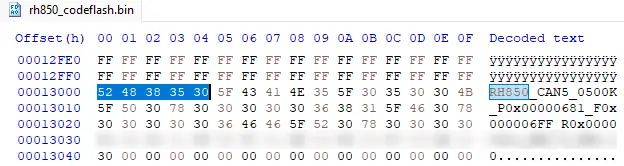
As mentioned above the 2 wire uart protocol communication happens over a series of commands. Once the whole data from code flash and data flash was extracted, we compared the checksum of the data received and packed the data into a binary file by removing the command metadata used by RFP tool as shown in the below figure.
After extracting both the code flash and data flash, we proceeded with reverse engineering the binary to find other vulnerabilities or obtain any other confidential information such as keys etc.
Conclusion
In this blog we showed how voltage glitching attack can be used to extract firmware from Read Protected MCU. A summary of the key findings are described below:
- Successfully bypassed 16-byte ID Code authentication to extract firmware.
- Reverse engineering the firmware, we obtained secret keys, used to unlock Secure Diagnostic Services.
- With the security access now bypassed, we could control vehicle actions.
All the vulnerabilities were privately disclosed to the Manufacturer and were patched. Details regarding vulnerabilities obtained during firmware reversing could not be disclosed to maintain confidentiality